
Last updated: 2026
Buck converter instability is one of the most common and most misdiagnosed problems in embedded and power electronics. Engineers spend days adjusting compensation values when the real issue is a capacitor, or they respin a PCB when the problem was a single poorly routed trace.
This article covers every real cause, with accurate DSO waveform references, a block diagram, PCB layout illustration, and a complete troubleshooting flowchart. All content is original and based on practical bench behaviour.
How a Buck Converter Works
A buck converter reduces a higher DC input to a lower regulated DC output by rapidly switching a MOSFET, then filtering the result through an inductor and capacitor. A feedback loop continuously compares the output to a reference voltage and adjusts the duty cycle to keep Vout stable.
Every instability problem traces back to something going wrong in this closed loop.
.png)
The blue path is the power flow. The orange path is the feedback loop. Instability always originates somewhere in this system either the power components, the compensation network, or the PCB layout.
Waveform 1: Inductor Current (Normal vs Saturating)
Clip a current probe around the inductor body. In healthy CCM operation you see a clean triangular wave. When the inductor saturates, the triangle top gets clipped flat inductance collapses mid-cycle and current rises uncontrolled.
.png)
The flat top is a definitive signature — no other waveform looks like this. Check both the RMS thermal rating and the saturation current rating on the inductor datasheet. Both must be within spec.
Waveform 2: SW Node (Clean vs Ringing)
Probe the switching node between the MOSFET and the inductor. Use a 10x probe with at least 200 MHz bandwidth and a short ground spring clip never a long croc lead.
.png)
The ringing frequency at each edge is set by the parasitic loop inductance resonating with the MOSFET output capacitance. On a real board this ringing couples into the feedback trace, adds noise to the regulated output, and can exceed the MOSFET Vds rating over time.
Waveform 3: Output Ripple Shape
Probe Vout directly across the output capacitor with AC coupling. The shape triangular or spikey tells you the dominant cause immediately.
.png)
The ESR spike appears at exactly each switching transition because the inductor current ramp reverses direction and the step-change in current through the capacitor's ESR creates an instantaneous spike: V = ESR × ΔI. Fix: switch to a polymer electrolytic capacitor, or add a 100 nF–1 µF MLCC in parallel.
Waveform 4: Load Transient Response
Switch a load resistor in and out while watching Vout at 50–200 µs/div. This is the fastest way to assess phase margin without a Bode plot analyser.
.png)
Target is the left screen small undershoot, clean recovery within 2–3 switching cycles, no sustained ringing. If you see the centre pattern, adjust the compensation R and C values on the COMP/FB pin per your IC datasheet design procedure.
The 7 Root Causes:
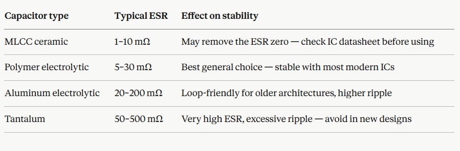
Cause 1 - Wrong or degraded output capacitor
The output capacitor's ESR is not just a ripple spec. For many controller architectures — particularly older voltage-mode controllers — the ESR provides a phase-lead zero in the feedback loop. Removing it by swapping to a low-ESR ceramic MLCC without updating the compensation network is one of the most common ways to introduce oscillation.
Capacitor typeTypical ESREffect on stabilityMLCC ceramic1–10 mΩMay remove the ESR zero check IC datasheet before usingPolymer electrolytic5–30 mΩBest general choice stable with most modern ICsAluminum electrolytic20–200 mΩLoop-friendly for older architectures, higher rippleTantalum50–500 mΩVery high ESR, excessive ripple avoid in new designs
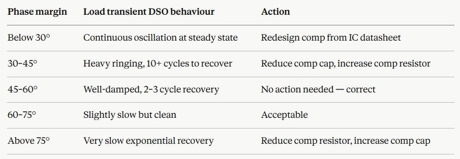
Cause 2 - Insufficient phase margin
Phase margin is the stability reserve in the closed-loop feedback system. Below 45° the output oscillates or rings heavily on load steps. Above 70° the loop is stable but sluggish.
Phase marginWhat you see on the DSOBelow 30°Continuous oscillation at steady state30–45°Heavy ringing, 10+ cycles to recover from load step45–60°Well-damped, 2–3 cycle recovery — target rangeAbove 70°Very slow recovery, sluggish transient response
Cause 3 - Inductor saturation
When peak inductor current exceeds the rated saturation current, the core's permeability collapses and inductance drops sharply — sometimes to 20–30% of nominal. Current then rises much faster than the controller expects and regulation is lost.
Calculate peak current: Ipeak = Iload + (Vin − Vout) × D / (2 × L × Fsw)
If Ipeak exceeds the inductor's Isat rating, you need a physically larger inductor or a higher-rated core.
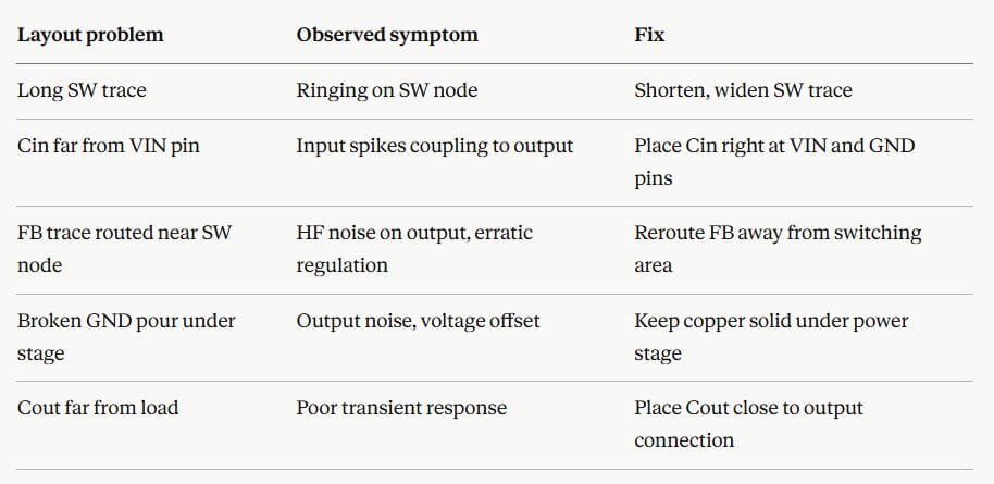
Cause 4 - PCB layout parasitics
Two paths are critical:
The hot switching loop from the input capacitor positive terminal, through the MOSFET, through the diode, back to the input capacitor ground. Every extra millimetre of trace adds roughly 1 nH of parasitic inductance. This resonates with circuit capacitances and produces SW node ringing.
The feedback trace the resistor divider and COMP pin connections sense a small voltage. Any switching noise coupled into this trace looks like a real Vout error and forces the controller to react.
Layout problemObserved symptomFixLong SW traceRinging on SW nodeShorten, widen SW traceCin far from VIN pinInput spikes coupling to outputPlace Cin right at VIN and GND pinsFB trace routed near SW nodeHF noise on output, erratic regulationReroute FB away from switching areaBroken GND pour under stageOutput noise, voltage offsetKeep copper solid under power stageCout far from loadPoor transient responsePlace Cout close to output connection
Cause 5 - Input voltage ripple coupling
Buck converters have finite input rejection. If the upstream supply has significant ripple, some leaks to the output. Test by adding 100 µF + 100 nF directly at the IC's VIN pins if output noise drops, the upstream supply is the problem.
Cause 6 - Thermal drift
Some controller ICs shift their current limit threshold, reference voltage, or oscillator frequency as junction temperature rises. A converter stable when cold but oscillating after 10 minutes is almost always a thermal problem. Use a heat gun on individual components while watching the DSO.
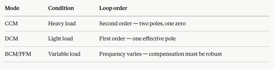
Cause 7- DCM/CCM boundary crossing
The converter's small-signal model changes significantly between CCM (heavy load) and DCM (light load). Compensation designed for one mode can be unstable in the other.
ModeConditionLoop orderCCMHeavy loadSecond order — two poles, one zeroDCMLight loadFirst order one effective poleBCM/PFMVariable loadFrequency varies compensation must be robust
PCB Layout: The Hot Switching Loop
.png)
Keep the hot loop copper area under 2 cm² on a 2-layer board. On a 4-layer board with a dedicated ground plane the parasitic inductance is much lower, but component placement order still matters — Cin must be closest to the IC.
Troubleshooting Flowchart
.png)
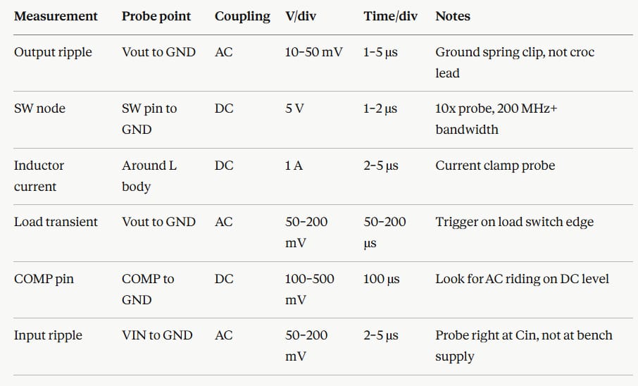
Complete Reference Tables
DSO settings for each key measurement
Five Bench Tips That Save Time
1. Use a ground spring clip, not a croc lead. A 10 cm croc-clip ground lead adds 10–20 nH to the probe circuit. At 500 kHz that creates apparent ringing in every measurement that does not exist in the real board. Always use the short coil spring that clips to the probe barrel.
2. Rule out the probe before blaming the circuit. Short the probe tip to its own ground and observe the noise floor. If you see activity, the probe or ground lead is the problem.
3. Measure Cout ESR with an LCR meter. Electrolytic capacitors degrade with temperature cycling. A degraded cap can measure correct capacitance but have ESR three to five times its original value. A basic LCR meter catches this in seconds.
4. On any new PCB spin, suspect layout before changing component values. A design that simulated correctly but misbehaves on the first real board is almost always a layout problem, not a schematic error.
5.Read your IC datasheet compensation procedure from start to finish. Most modern buck controller datasheets include a step-by-step compensation calculation with component equations. Most new-design instability comes from skipping this and copying values from a reference design that used different capacitors and inductors.
Key Takeaways
Output instability in a buck converter almost always comes from one of three places: the output capacitor type or value, the compensation network, or the PCB layout. The DSO waveform shape tells you which category to investigate before touching anything. A triangular ripple with spikes points to ESR or layout. A clean ripple with ringing on load steps points to compensation. A flat-top inductor current waveform is definitive saturation. Run the eight-step sequence in order and you will find the cause on every board.


