
Last updated: 2026
Introduction: The Tiny Component with a Massive Job
You've probably heard it a hundred times in electronics design: "Place your decoupling caps as close as possible to the IC power pin." But have you ever stopped to ask why? What actually happens if you don't? Is it just a best-practice myth passed down from old textbooks, or is there hard physics behind it?
Spoiler: There is very hard physics behind it. And once you understand it, you'll never again route a power trace carelessly around a bypass capacitor.
In this article, we're going to break down the full science from parasitic inductance to impedance resonance, backed by real numbers, waveforms, and examples. By the end, you'll not only understand why proximity matters, but you'll also know exactly how to do it right on your next PCB.
What Is a Decoupling Capacitor, Really?
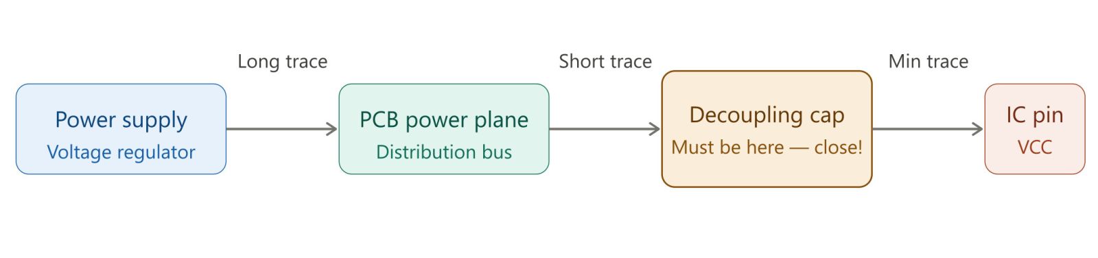
A decoupling capacitor (also called a bypass capacitor) is placed between the VCC and GND pins of an IC, as close as physically possible to the supply pin. Its job is to act as a local, on-demand energy reservoir.
When a digital IC switches a microcontroller toggling an output pin, an FPGA switching millions of gates it demands a sudden burst of current in nanoseconds. The main power supply, sitting centimeters away, simply cannot respond fast enough. The decoupling capacitor steps in and supplies that charge locally, almost instantaneously.
.jpg)
The Real-Life Analogy: The Rooftop Water Tank
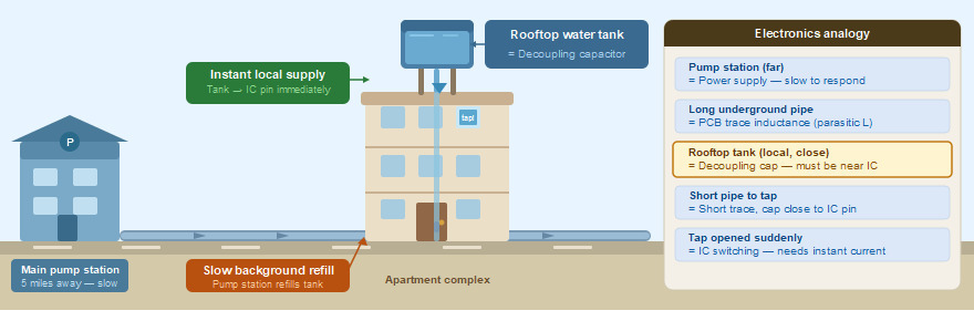
The pump station (far left) = your power supply (VCC), sitting far away and slow to react. The underground main pipe = the long PCB trace with high inductance. The rooftop water tank = your decoupling capacitor, sitting right at the building (IC). The short internal pipe = the short trace from cap to IC pin. The tap being opened = the IC switching and demanding sudden current.
The green label shows the instant local supply from the rooftop tank, and the orange label shows the slow background refill from the distant pump station exactly mirroring how a decoupling cap and power supply work together.
The Real Enemy — Parasitic Inductance
Here is the core reason why distance kills decoupling performance: every trace on a PCB has inductance. Any conductor carrying current creates a magnetic field, and that field stores energy. That energy storage is inductance.
The inductance of a PCB trace can be estimated by:
L ≈ 2 × length × [ln(2 × length / width) − 0.75] nH (length and width in cm)
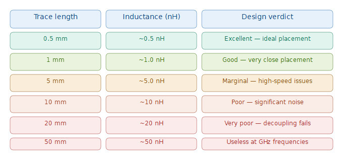
For practical PCB work, the rule of thumb is simple:
~1 nH per millimeter of trace length
Impedance — The Whole Game
To understand why inductance is so bad, we need to talk about impedance. Impedance (Z) is the opposition to the flow of current in an AC circuit. Unlike resistance, it changes with frequency.
For an inductor: Z_L = 2π × f × L
For a capacitor: Z_C = 1 / (2π × f × C)
A real decoupling capacitor is not just a capacitor. It's a capacitor in series with parasitic inductance (ESL) and resistance (ESR) forming a real-world RLC series circuit:
Z_total = √[ ESR² + (2πfL − 1/2πfC)² ]
This impedance has a very specific and critical shape when plotted against frequency:
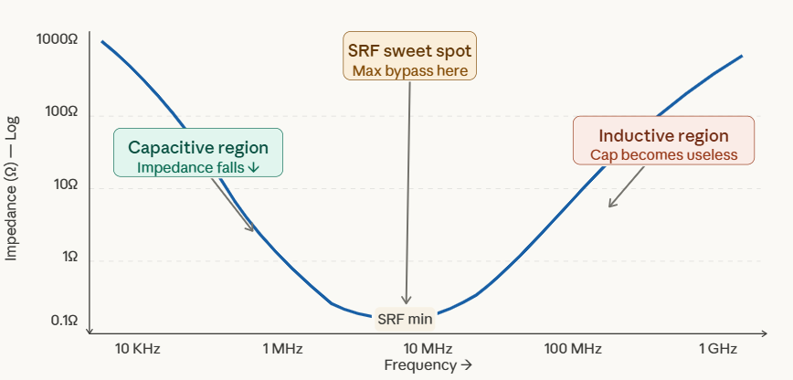
The curve above tells the whole story. Below the Self-Resonant Frequency (SRF), the capacitor does its job impedance falls as frequency rises. At the SRF, impedance is at its absolute minimum (limited only by ESR). Above the SRF, the parasitic inductance takes over impedance rises, and the capacitor becomes progressively useless.
When you move the cap away from the IC pin, you add inductance, which pushes the SRF downward shrinking the useful frequency window.
Numerical Example — The Cost of Distance
Let's run real numbers. We have a 100 nF decoupling capacitor with ESR = 0.05 Ω and ESL (intrinsic) = 1.0 nH.
Self-Resonant Frequency of the capacitor itself:
SRF = 1 / (2π × √(L × C))
SRF = 1 / (2π × √(1×10⁻⁹ × 100×10⁻⁹))
SRF ≈ 15.9 MHz
Now watch what happens as we add trace length:
Add 5 mm of trace (≈ 5 nH extra): Total L = 6 nH → New SRF ≈ 6.5 MHz
Add 20 mm of trace (≈ 20 nH extra): Total L = 21 nH → New SRF ≈ 3.5 MHz
A cap designed to work at 15.9 MHz is now barely useful above 3.5 MHz just because of 20 mm of extra trace. If your IC switches at 100 MHz, this capacitor is doing essentially nothing.
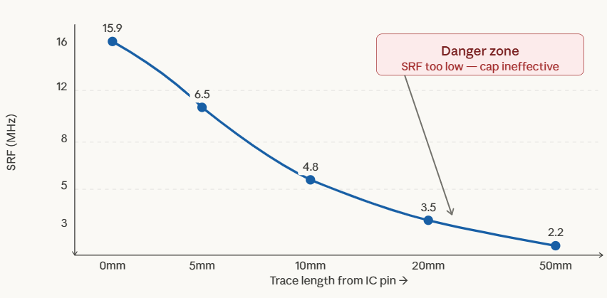
The SRF curve drops steeply as trace length increases — most of the damage happens in the first 10 mm. This is why the rule is not "place it reasonably close" but "place it as close as physically possible."
Voltage Droop — What Actually Happens at the IC Pin
When the decoupling capacitor can't deliver charge fast enough due to high inductance, the IC's supply voltage droops. The formula is:
ΔV = L × (ΔI / Δt)
Let's use a realistic example: an IC demands a current step of ΔI = 100 mA in Δt = 1 ns (typical for a 500 MHz digital IC):
Cap at 1 mm (L = 1 nH): ΔV = 1×10⁻⁹ × (0.1 / 1×10⁻⁹) = 0.1 V — acceptable
Cap at 10 mm (L = 10 nH): ΔV = 10×10⁻⁹ × (0.1 / 1×10⁻⁹) = 1.0 V — catastrophic on a 3.3 V supply (30% fluctuation!)
A 1.0 V droop can cause logic glitches, corrupt flip-flop data, trigger false resets, and violate setup/hold timing. Here is what the voltage waveform at the IC pin looks like in both cases:
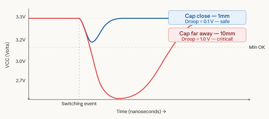
The blue waveform shows a small, fast-recovering droop when the cap is close. The red waveform shows what happens when it's 10 mm away — a massive voltage collapse that takes many nanoseconds to recover. If another switching event happens during that recovery, the IC is operating in completely unpredictable territory.
The Loop Area Problem — EMI and Radiation
When the capacitor is placed far from the IC pin, the current path forms a large loop. According to Maxwell's equations, a current-carrying loop of area A radiates electromagnetic energy proportional to:
E ∝ f² × I × A
The far capacitor creates a loop that could be 150× larger in area. Since EMI scales with area, this can translate to 150× more radiated noise the difference between passing and catastrophically failing an EMC test.
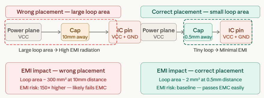
The loop area difference between the two placements is enormous. Every doubling of loop area doubles the radiated EMI. A cap 10 mm away versus 0.5 mm creates a loop that's approximately 150× larger that is the difference between passing an EMC test and failing it by a wide margin.
The Via Problem — Extra Inductance You Forgot About
If your decoupling capacitor is on the bottom layer and the IC is on the top layer, the current must travel through vias to reach the power plane. Each via adds approximately 0.3 to 1.0 nH of inductance, depending on board thickness and via diameter.
Via inductance estimation:
L_via ≈ 5.08 × h × [ln(4h/d) + 1] nH (h and d in inches)
For a standard 1.6 mm board with a 0.3 mm drill: h = 0.063", d = 0.012"
L_via ≈ 0.32 × [ln(21) + 1] ≈ 1.3 nH per via
Two vias in the decoupling path add ~2.6 nH — equivalent to 2.6 mm of extra trace. Here is how the via count affects the total inductance budget:
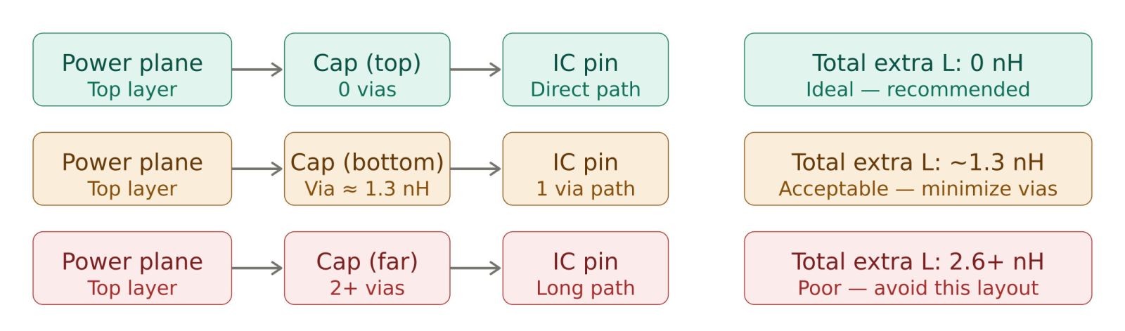
The golden rule on vias: use the minimum possible (zero is best), keep them close to the capacitor pads, and use wide, short via holes to minimize their individual inductance.
Capacitor Value Selection — The Frequency Hierarchy
Different capacitor values cover different frequency ranges. This is why professional PCB designs use multiple capacitors in parallel a strategy called the capacitor hierarchy. Using only one value leaves large frequency gaps in your power delivery coverage.
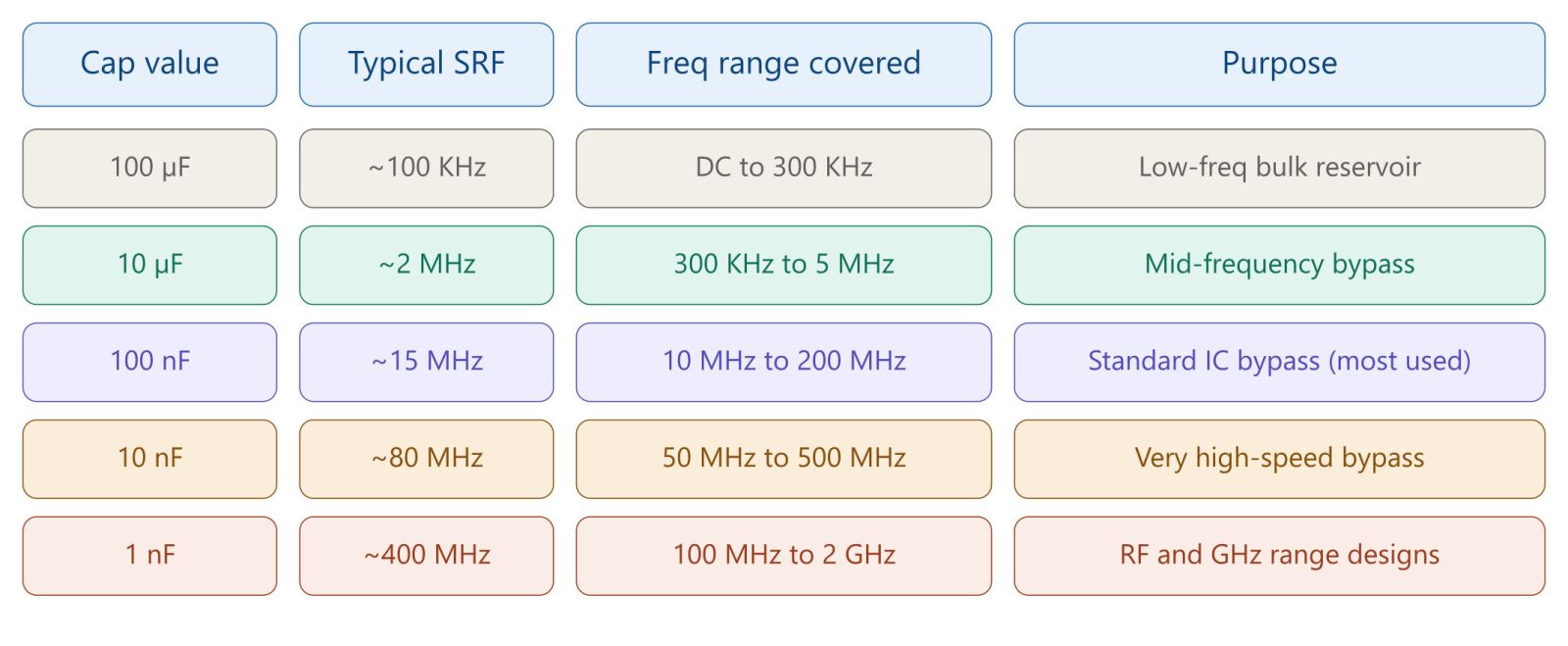
A 100 nF and 10 nF capacitor placed together cover a much wider frequency band than either one alone. This is the standard two-cap strategy for most digital ICs. For RF or high-speed designs, adding a 1 nF cap covers everything up to 2 GHz.
Visualizing the Impact: The Waveform Analysis
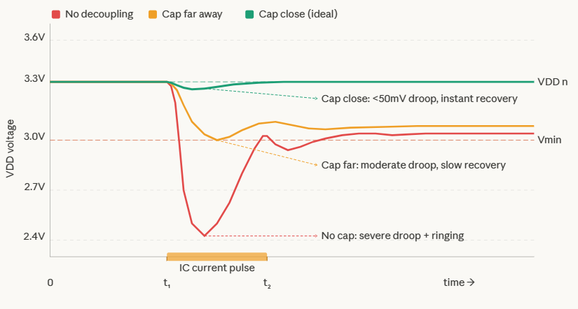
During a fast switching event (t1 to t2), the IC draws a sudden current pulse. How well your capacitor supports this depends on its placement:
-
Green Path (Cap Close): Minimal voltage drop (<50 mV), fast recovery → stable operation
-
Yellow Path (Cap Far): Noticeable droop, slow recovery → risk of instability
-
Red Path (No Cap): Large voltage drop + ringing → failures, resets, EMI issues
Key takeaway: The closer the decoupling capacitor is to the IC, the more stable your system will be.
Anti-Resonance — The Hidden Danger of Parallel Caps
When you place two capacitors in parallel, something interesting and potentially dangerous happens at a specific frequency: anti-resonance. At this frequency, the inductive behavior of the smaller capacitor (already past its SRF) combines with the capacitive behavior of the larger one to create a high-impedance spike on the power rail.
Anti-Resonance Frequency:
f_anti = 1 / (2π × √(L_small × C_large))
For a 100 nF cap (ESL = 1 nH) with a 10 nF cap (ESL = 0.5 nH):
f_anti ≈ 1 / (2π × √(0.5×10⁻⁹ × 100×10⁻⁹)) ≈ 712 MHz
At 712 MHz, the parallel combination creates a peak in impedance rather than a dip. If your IC generates noise at this exact frequency, it will see a high-impedance supply rail — the opposite of what you wanted.
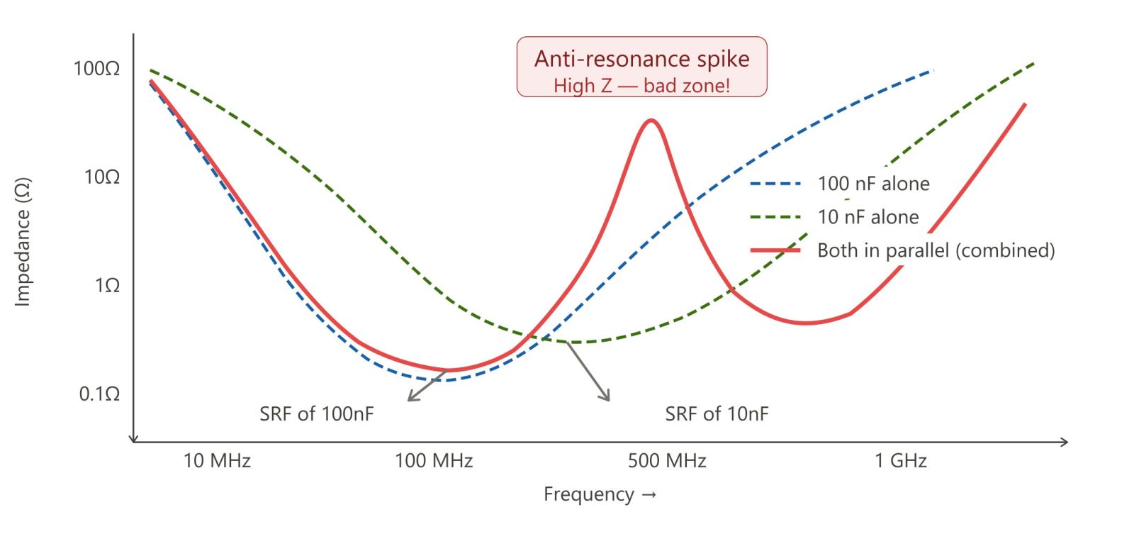
Notice the red combined curve: it has a sharp impedance spike between the two SRF dips. This is anti-resonance. The solution is to choose capacitor values whose SRFs are close together, or add a ferrite bead in series to damp the resonance. Using capacitors from the same package family with similar ESL also helps.
Practical PCB Layout Rules — Do This Every Time
Here is the complete set of golden rules backed by everything discussed so far:
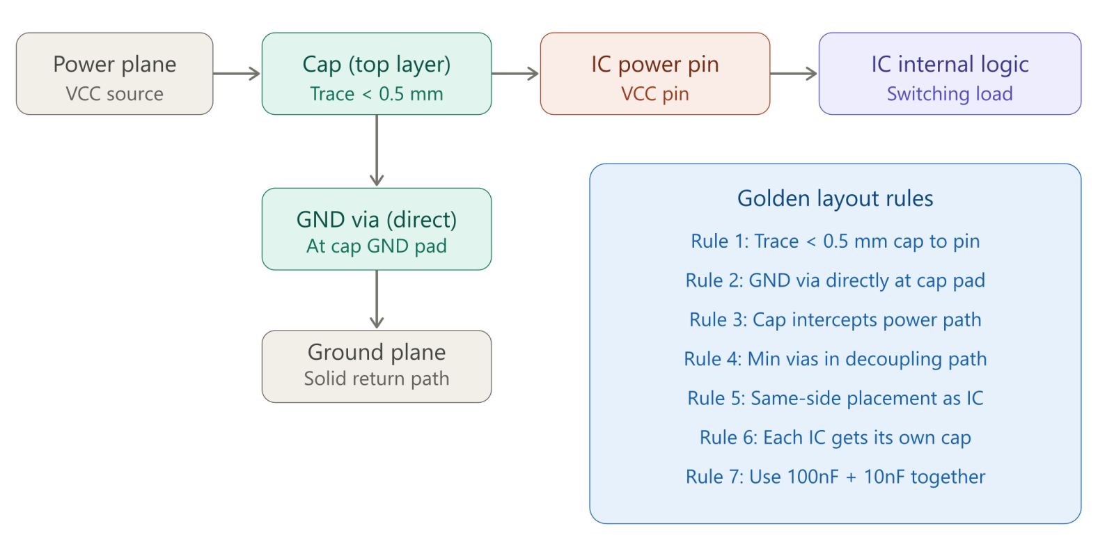
The flow on the left shows the ideal current path: power plane feeds the capacitor, capacitor feeds the IC pin, and the GND side of the cap goes directly down through a via to the ground plane. No detours. No shared vias. No long traces.
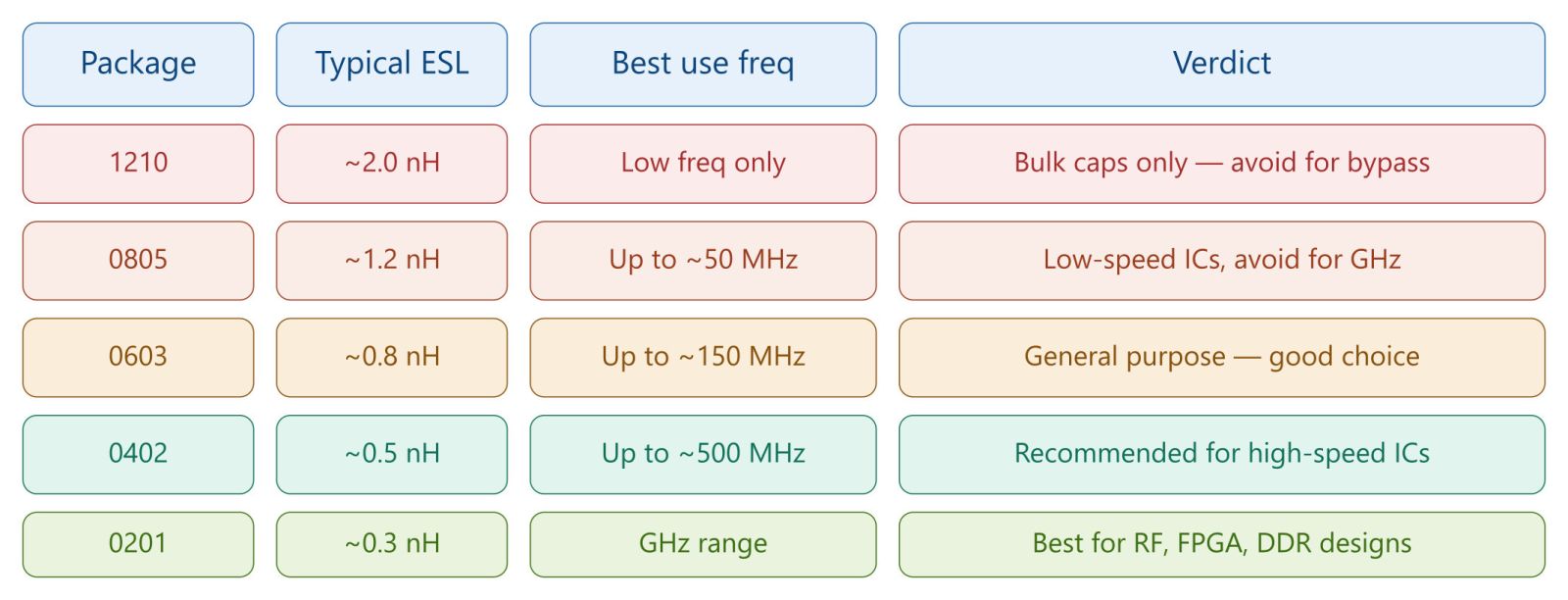
Package Size Matters — Smaller is Better at High Frequencies
Smaller capacitor packages have lower ESL. For high-frequency decoupling, the package choice is as important as the capacitor value itself:
Real-World Case Study — STM32F4 Microcontroller
The STM32F4 series runs at up to 168 MHz internal clock with switching edges well under 1 ns. ST's own datasheet recommends one 2.2 µF ceramic per VDD pin group, one 100 nF ceramic per VDD pin (placed as close as possible), and a 1 µF plus 10 nF combination on the VDDA analog supply pin.
Let's validate using our voltage droop formula for a 200 mA current step in 0.5 ns:
Cap at 0.3 mm (L ≈ 0.3 nH): ΔV = 0.3×10⁻⁹ × (0.2/0.5×10⁻⁹) = 0.12 V — safe
Cap at 1 mm (L ≈ 1 nH): ΔV = 1×10⁻⁹ × (0.2/0.5×10⁻⁹) = 0.4 V — borderline
Cap at 5 mm (L ≈ 5 nH): ΔV = 5×10⁻⁹ × (0.2/0.5×10⁻⁹) = 2.0 V — catastrophic on a 3.3 V supply
This is exactly why ST's own reference designs show the decoupling capacitors literally touching the IC pads, with GND vias placed immediately adjacent to the capacitor ground pads. That's not aesthetics that's physics.
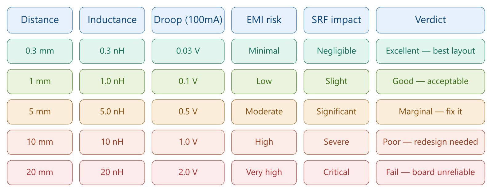
Final Summary: Consequences at a Glance
Conclusion: Proximity Is Not a Suggestion — It's Physics
Let's bring everything together. A decoupling capacitor must be placed close to the power pin because:
Every millimeter of trace adds ~1 nH of inductance, which directly opposes sudden changes in current. Increased inductance lowers the Self-Resonant Frequency, shrinking the effective frequency range of the capacitor. Voltage droop scales linearly with inductance — a cap at 10 mm causes 10× more droop than one at 1 mm. A larger current loop creates more EMI radiation, potentially causing your board to fail EMC testing. Anti-resonance effects from multiple caps are made worse by trace inductance. And every via in the decoupling path adds another ~1.3 nH that you did not budget for.
Whether you are designing a simple Arduino shield or a high-speed FPGA board at 500 MHz, the rules don't change. Place your decoupling capacitors as close as physically possible to the VCC pin. Use a direct ground via right at the cap's GND pad. Follow the capacitor hierarchy for wide-band coverage. Choose 0402 or 0201 packages for anything above 50 MHz.
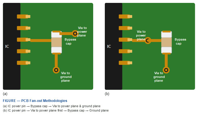
(a) Correct approach — The power trace from the IC pin hits the bypass capacitor first, then continues to the via for the power plane. The cap intercepts the current path directly.
(b) Incorrect approach — The power trace goes to the via first, then to the bypass cap as a stub. The cap is now off the main current path and much less effective.


