
Last updated: 2026
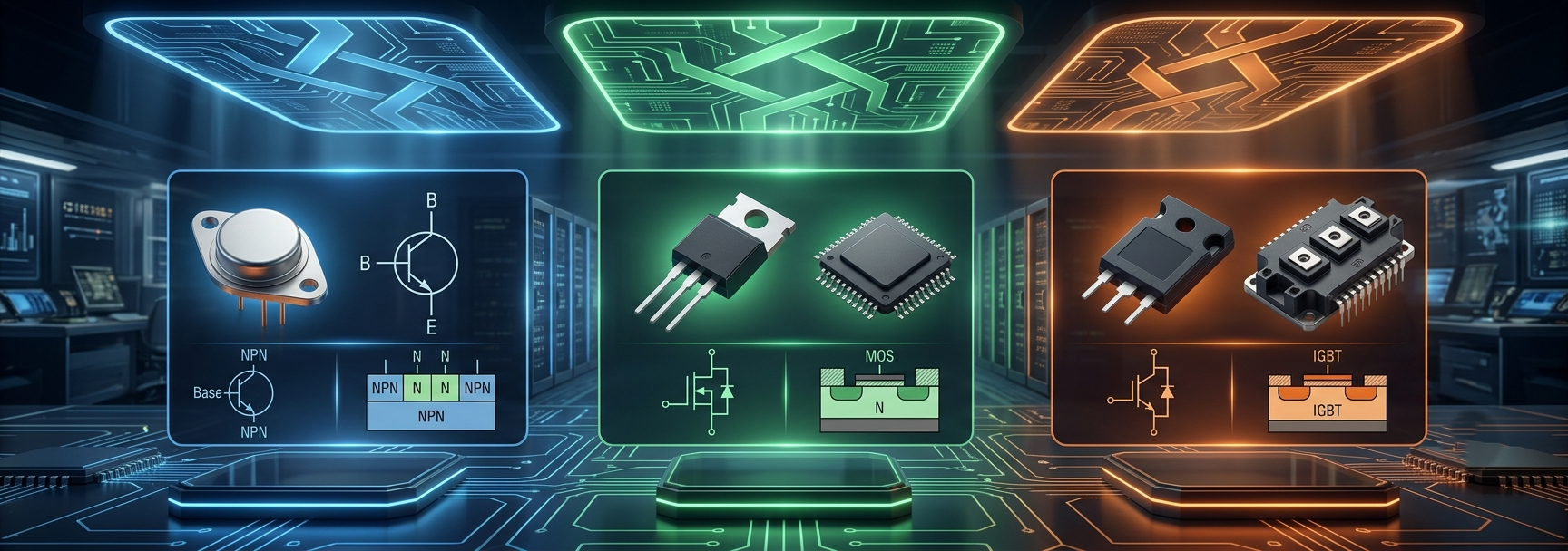
When designing a switch-mode power supply (SMPS), motor drive controller, or solar inverter, electrical engineers face a foundational architectural choice: Which power semiconductor switch is right for the application? Selecting between a BJT (Bipolar Junction Transistor), a Power MOSFET (Metal-OxideSemiconductor Field-Effect Transistor), and an IGBT (Insulated Gate Bipolar Transistor) dictates the system's thermal management infrastructure, operational efficiency, physical footprint, and overall bill of materials (BOM) cost.
1. Bipolar Junction Transistor (BJT): The Current-Driven Classic
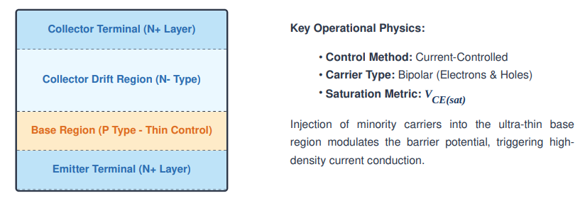
The power BJT is a three-layer (NPN or PNP) legacy semiconductor device. While predominantly superseded by voltage-controlled alternatives in modern high-frequency circuits, it remains highly viable for cost-sensitive, low-frequency, low-power switching applications.
Internal Physical Architecture
Core Operating Principles
The BJT operates inherently as a current-controlled device. To command and sustain an active current channel from the Collector to the Emitter (IC ), a continuous, proportional base current (IB ) must be continuously forced into the Base node. In the linear active zone, this is governed by the DC current gain (β):
IC = β × IB
To limit conduction power dissipation, a power switching circuit must drive the BJT fully past the active region and deep into saturation. In hard saturation, both internal junctions become fully forward-biased, shrinking the collector-to-emitter forward voltage drop to its structural limit, denoted as VCE(sat) (typically 0.2V to 0.4V).
Reference Application Circuit: 12V Solenoid & Relay Driver
This industrial configuration permits a standard low-power 5V microcontroller GPIO pin to reliably switch a high-current 12V inductive load via an NPN power BJT.
.png)
Step-by-Step Engineering Calculations
To ensure the TIP31C transistor functions with optimal efficiency as a pure switch, the base network must guarantee continuous full saturation across load and temperature variations.
1. Calculate Nominal Collector Current (IC ):
IC = (VCC - VCE(sat)) / RL = (12 V - 0.2 V) / 300 Ω = 39.33 mA
2. Determine Required Base Current (IB ) Under Forced Beta Conditions:
While standard datasheets show high linear DC gains, gain drops sharply under saturation. Engineers employ a conservative forced beta (β sat) rule-of-thumb value between 10 and 15:
IB = IC / βsat = 39.33 mA / 15 = 2.62 mA
3. Size the Base Current Limiting Resistor (RB ):
Given a 5V microcontroller logic input level and an internal base-emitter forward saturation drop (VBE(sat)) of 0.7V:
RB = (Vin - VBE(sat)) / IB = (5 V - 0.7 V) / 2.62 mA = 4.3 V / 0.00262 A ≈ 1641 Ω
Engineering BOM Selection: To guarantee hard saturation across all component tolerances, select a standard 1.5 kΩ resistor. This comfortably increases the operational base drive current to 2.86 mA, ensuring a crisp transition without overstressing the microcontroller's GPIO pin.
2. Power MOSFET: The High-Speed Speed Demon
The Power MOSFET revolutionized modern high-frequency power electronics conversion. Utilizing a vertical DMOS configuration instead of the lateral designs seen in signal microchips, it handles high current densities and blocks high reverse voltages across an extensive drift zone.
Internal Physical Architecture
The defining feature of a MOSFET is its entirely insulated control gate, isolated from the semiconductor body by an ultra-thin layer of silicon dioxide (SiO2 ).
.png)
Core Operating Principles
The Power MOSFET functions purely as a voltage-controlled, unipolar device. When a gate-to-source bias (VGS) exceeding the threshold voltage (Vth) is applied, an electrostatic field draws electrons to form a channel. Because conduction relies strictly on majority carriers, the device completely bypasses minority carrier storage delays during turn-off transitions. When fully turned on, the internal conduction path operates explicitly as a linear resistor, designated as RDS(on). Conduction losses scale quadratically with current:
P_loss = ID(RMS)^ 2 × RDS(on)
Reference Application Circuit: High-Speed PWM DC Motor Controller
This configuration implements high-frequency Pulse Width Modulation (PWM) to regulate the speed of a highpower DC motor smoothly and efficiently.
.png)
Step-by-Step Engineering Calculations
Using the industry-standard IRF540N MOSFET, we calculate the continuous thermal load and dynamic gate drive metrics for a 10A current load.
1. Calculate Conduction Power Loss (Pcond):
The IRF540N features a maximum on-state channel resistance (RDS(on)) of 44 mΩ at a standard gate voltage of 10V
P_cond = ID^ 2 × RDS(on) = (10 A)^2 × 0.044 Ω = 100 × 0.044 = 4.4 W
Thermal Design Insight: A continuous dissipation of 4.4W will quickly cause overheating. A small TO-220 aluminum heatsink rated for ≤ 10°C/W is required to keep the internal silicon junction temperature safely below its 175°C maximum.
2. Calculate Dynamic Gate Drive Current Requirements (Ig(peak)):
While the gate draws zero steady-state DC current, the input capacitance must be quickly charged to pass through the high-loss linear region. The datasheet lists a Total Gate Charge (Qg ) of 71 nC. To hit a crisp target transition rise-time (Δt) of 50 ns:
Ig(peak) = Qg / Δt = 71 nC / 50 ns = 1.42 A
Because standard microcontroller GPIO pins cannot supply 1.42A pulse bursts, a dedicated high-current gate driver IC (such as a Microchip TC4427) must be placed between the MCU and the 10Ω gate series resistor.
3. Insulated Gate Bipolar Transistor (IGBT): The Heavyweight Hybrid
The IGBT is an advanced functional hybrid component. It unifies the easy-to-drive, high-input impedance gate of a MOSFET with the low-voltage-drop, high-current density conduction output of a bipolar junction transistor.
Internal Physical Architecture
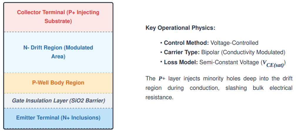
Structurally, the IGBT closely mirrors a vertical MOSFET, but incorporates an essential addition: a heavily doped P+ substrate layer at the collector interface.
Core Operating Principles
When a positive gate-emitter bias (VGE) is applied, the internal MOSFET structure channels current into the base of an embedded PNP bipolar transistor structure. This initiates conductivity modulation: minority carriers continuously flood the wide drift region, slashing the bulk silicon resistance under high-voltage scenarios. Consequently, instead of scaling exponentially with voltage like a MOSFET, the IGBT output acts like a standard forward diode with a relatively stable, predictable forward saturation voltage drop (VCE(sat)):
P_cond ≈ IC × VCE(sat)
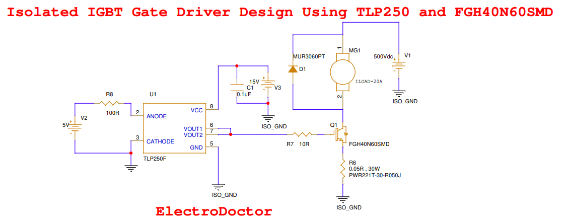
Reference Application Circuit: Isolated IGBT Gate Driver Design Using TLP250 and FGH40N60SMD
This architecture forms one out of three primary phase legs utilized to construct a variable frequency drive (VFD) for AC motor actuation, or can be adapted for grid-tie solar inverter installations and high-power DC motor control as shown in the schematic.
Step-by-Step Engineering Calculations
We assess the performance of the 600V, 40A Field Stop IGBT (FGH40N60SMD) running a continuous load current ILOAD of 20A on a 500V DC rail.
Calculate High-Voltage Conduction Loss (P_cond)
As Per the FGH40N60SMD datasheet operational characteristics, at the specific application load current of 20A, the forward collector-emitter saturation voltage (VCE(sat)) sits at approximately 1.5V:
P_cond = Ic x VCE(sat) = 20 A x 1.5V = 30W
4. Head-to-Head Architectural Parameter Comparison
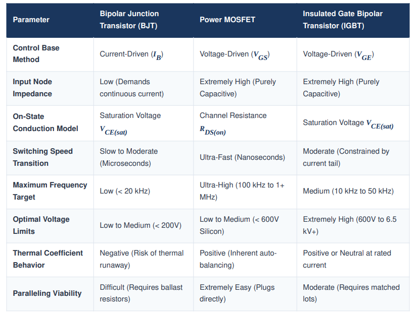
5.The Application Selection Matrix
.png)
Final Engineering Selection Blueprint:
• Deploy a BJT (e.g., TIP31C): For basic, cost-constrained, low-frequency configurations where continuous control drive current is acceptable.
• Deploy a MOSFET (e.g., IRF540N): For lower voltage domains (< 600V) that demand ultra-fast, high-efficiency operations (e.g., DC-DC converters, synchronous rectification).
• Deploy an IGBT (e.g., FGA25N120ANTD): For rugged high-voltage systems (> 600V) switching massive inductive currents at moderate frequencies (e.g., inverters, heavy motor controllers).