Last updated: 2026
A working schematic is not a working product. You can have the right chip, right firmware, and right power supply. But if the PCB layout is wrong, the board still fails. Sometimes on day one, sometimes six months later in a customer's hands. That second case is the expensive one.
These are the ten layout mistakes that cause the most field failures, EMI test failures, and re-spins. Every one of them has caused real product recalls and dead prototypes.
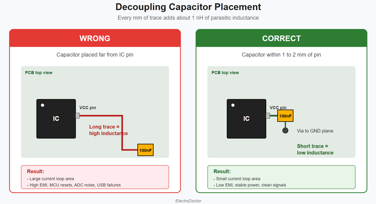
1. Decoupling Capacitors Placed Too Far From the IC
A decoupling capacitor only works if it is electrically close to the IC power pin. Every millimetre of trace adds roughly 1 nH of parasitic inductance, which kills the capacitor's high-frequency performance.
What goes wrong: Random MCU resets, ADC noise, USB enumeration failures, failed EMI scans.
The rule:
-
Place the smallest capacitor (100 nF) within 1 to 2 mm of the power pin.
-
Connect to power and ground planes through short, direct vias, not long traces.
-
Keep the loop area between capacitor, IC, and return path as small as possible.
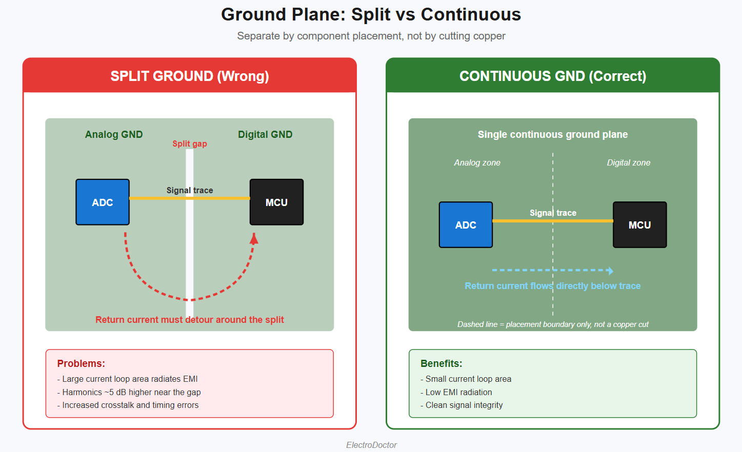
2. Splitting the Ground Plane (When You Shouldn't)
For years, designers were told to split ground planes into analog and digital sections. In most modern designs, this advice is wrong.
When a digital signal crosses the gap between two ground islands, the return current cannot follow. It detours around the split, creating a large loop that radiates EMI. Traces crossing a ground plane gap show harmonics roughly 5 dB higher than traces over solid ground.
The fix:
-
Use a single continuous ground plane.
-
Separate analog and digital sections by component placement, not by cutting the copper.
-
Only split for very low-frequency precision analog (below 100 kHz) or galvanic isolation.
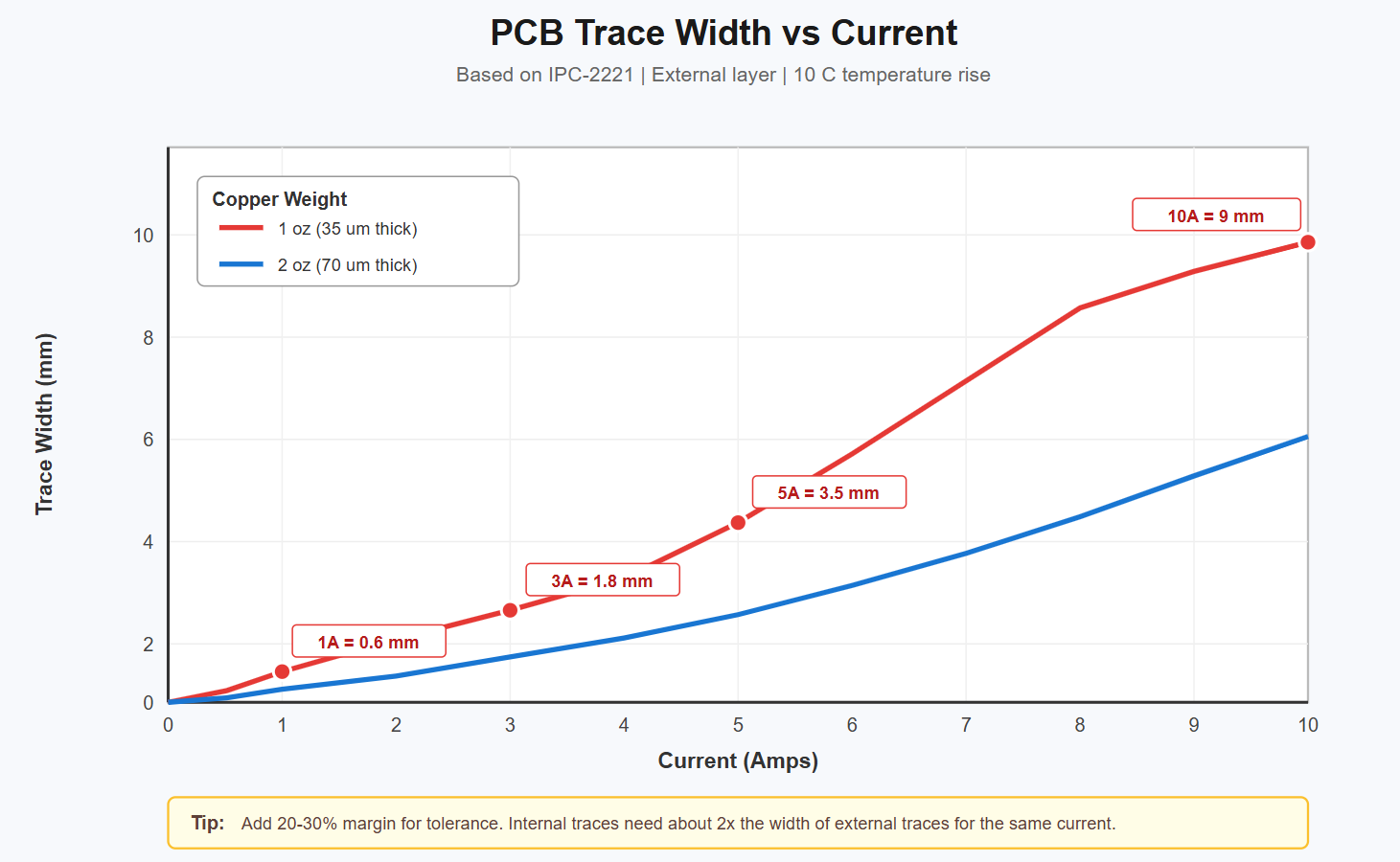
3. Trace Widths That Cannot Handle the Current
A trace is a resistor. Push too much current through a thin trace and it heats up, lifts off, or burns like a fuse.
Quick reference (1 oz copper, 10 °C rise, external trace, per IPC-2221):
CurrentTrace Width1 A0.6 mm (24 mil)3 A1.8 mm (70 mil)5 A3.5 mm (138 mil)10 A9 mm (350 mil)
Tips:
-
Use an IPC-2221 calculator before drawing power rails.
-
Add 20 to 30 percent margin for tolerance and surges.
-
Internal traces need roughly twice the width of external traces for the same current.
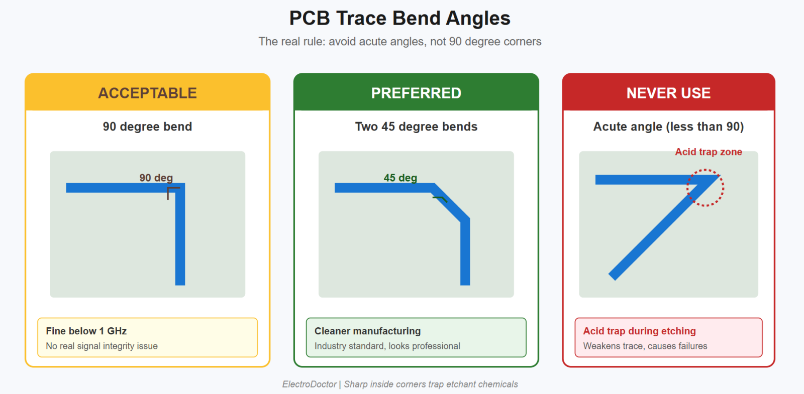
4. Acute Angles in Traces
The popular claim that 90-degree corners cause signal reflections is mostly wrong below 1 GHz. The real problem is acute angles (less than 90 degrees). They create acid traps during etching, weakening the trace.
The rule:
-
90-degree bends are acceptable for most designs.
-
45-degree bends are preferred and look cleaner.
-
Acute angles are never acceptable.
-
For signals over 5 GHz, use curved traces.
5. No Thermal Management for Hot Parts
-
Hot components fail. They degrade, drift, and die. The most common mistake is missing thermal vias under voltage regulators, MOSFETs, and processors.
-
The fixes:
-
Place a 4x4 or 5x5 thermal via array under any package rated above 1 W.
-
Use 0.3 mm drill, 0.6 mm pad, filled or plugged for reflow.
-
Connect to internal copper planes that spread heat.
-
Keep electrolytic capacitors at least 5 mm from regulators. Every 10 °C of extra temperature roughly halves their life.
.png)
6. Bad Component Placement
Layout software lets you place components anywhere. The autorouter will connect them. That does not mean it will work.
Common mistakes:
-
Crystals placed far from the microcontroller
-
High-current paths crossing the centre of the board
-
Tall components near edges that hit enclosure walls
-
Test points placed where you cannot reach with a probe
-
The rules:
-
Place critical components (crystals, decoupling caps, sensors) first. Route around them.
-
Keep crystal traces under 10 mm.
-
Group components by function: power, analog, digital, RF.
-
Think about assembly and repair access.
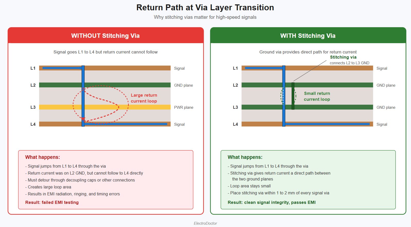
7. Return Path Discontinuities at Vias
When a signal moves between layers through a via, its return current must also find a path back. If the return current cannot follow, you get EMI and ringing.
The fix:
-
Add a ground stitching via next to every signal via that changes reference layers.
-
Never route fast signals over slots or splits in the ground plane.
-
For RF designs above 1 GHz, space stitching vias at less than one-tenth wavelength.
8. Wrong or Untested Component Footprints
This is the mistake that turns a clean layout into recycling. The schematic is right, the routing is clean, but the footprint is 0.5 mm off. Nothing fits.
Common failures:
-
Wrong package variant (QFN-32 5x5 vs 4x4)
-
Pin 1 marker on the wrong corner
-
Pad sizes that do not match IPC-7351
-
Reversed polarity markings on diodes or electrolytic caps
-
Prevention:
-
Verify every footprint against the manufacturer datasheet, not a library symbol.
-
Use IPC-7351 standard land patterns.
-
Print the layout at 1:1 scale and physically place components on paper before fab.
9. Skipping DRC and DFM Checks
Modern CAD tools have a Design Rule Check button. Many designers ignore the warnings.
What gets missed:
-
Trace-to-trace clearance violations
-
Drill-to-copper distance failures
-
Annular ring violations causing via breakout
-
Silk on pads blocking solder
-
The rules:
-
Run DRC before exporting Gerbers, every single time.
-
Load your specific manufacturer's DFM rules into your CAD tool.
-
Fix every warning, not just the errors.
-
One real case: 5,000 boards were scrapped because DRC had been disabled to "speed up" the export.
10. Bad Silkscreen and Missing Fiducials
This sounds cosmetic. It is not. Silkscreen mistakes cause assembly errors and field failures that look like real bugs.
Standards:
-
Minimum silkscreen text height: 0.8 mm (32 mil).
-
Clear pin 1 marker (dot or chamfer) on every IC.
-
Three fiducials in a non-symmetric pattern for SMT assembly.
-
Include board name, revision number, and date.
-
Real example: An assembly house populated 500 boards with all electrolytic capacitors reversed. The polarity marker was placed on the wrong pad in CAD. The boards looked perfect until power-on, then capacitors exploded.
Conclusion
You can pick the best components, write clean firmware, and still ship a broken product if the layout is wrong. The pattern is always the same: small layout decisions create big field failures, expensive recalls, and certifications that fail at the last minute.
Pre-fab checklist:
-
Decoupling caps within 2 mm of every power pin
-
Continuous ground plane, no splits under signal traces
-
Power trace widths calculated, not guessed
-
All bends 45 degrees or smoother, no acute angles
-
Thermal vias under every hot component
-
Stitching vias next to signal vias that change layers
-
Every footprint verified against the datasheet
-
DRC run with the actual manufacturer's DFM rules
-
Silkscreen readable, with fiducials and a revision number
-
If you can answer yes to all of them, your board has a much better chance of working on the first try.